Leadership
IBM’s Robert H. Dennard and the Chip That Changed the World
November 7, 2019 | Written by: John Markoff
Categorized: Leadership | Supercomputing | Systems
Share this post:
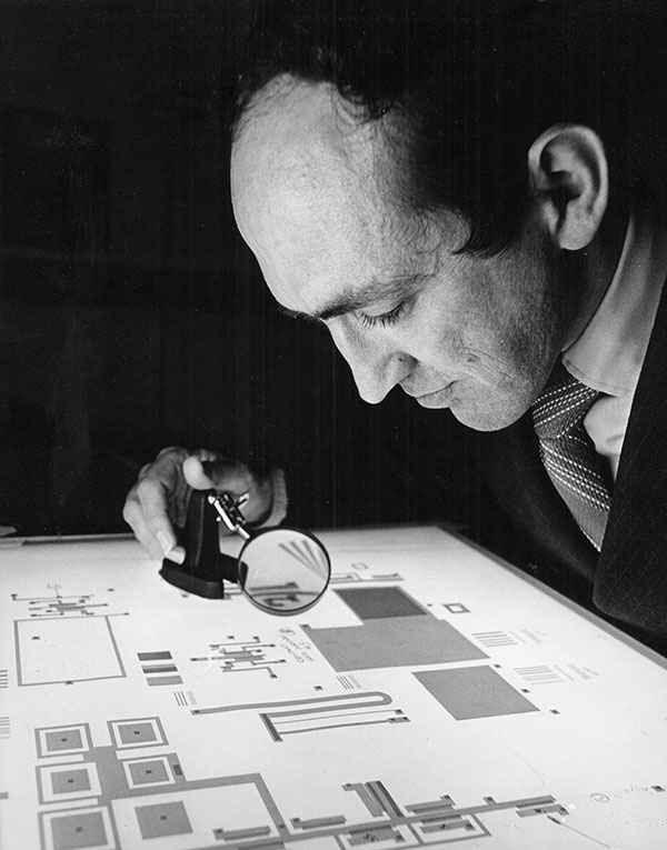
Robert H. Dennard
The inspiration, as is often the case, came late one evening. Bob Dennard, then a 34-year-old IBM electrical engineer, was pondering a colleague’s research presentation he’d seen earlier that day.
It was autumn 1966, and Dennard had been helping design a new form of computer memory using silicon-based transistors. This approach, known as microelectronics, would stand in contrast to the computer industry’s tradition of storing data magnetically – a technology referred to as core memory. The presentation that Dennard had listened to with a trace of envy was by a competing team of IBM engineers at work on new, smaller forms of magnetic storage.
Back then, the largest magnetic storage systems, requiring room-sized equipment, could store only one megabyte of information. That would be equivalent to a 500-page book – or about a minute of a Top 40 pop song. Besides being bulky, these storage systems were slow and they consumed huge amounts of electrical power. But now Dennard’s colleagues were describing a plan to shrink the next generation of magnetic memory to a compact 25-centimeter square.
Inspired, Dennard that evening wondered whether he could develop something equally simple and elegant – and probably much cheaper. His approach would involve semiconductor technology that used patterns of tiny wires, transistors and other components etched in silicon.
At the time, IBM’s silicon chip designers were wrestling with complex circuits that would use six transistors to store a single bit of data. They worked. But they were hardly efficient – and it didn’t seem a promising way to build systems capable of storing large volumes of data. But suddenly, that evening in 1966, Dennard had a flash of insight: You could store a bit with a single transistor!
To do so, he realized, would require using tiny amounts of energy to repeatedly refresh the capacitor that held the charge to store the bit. Otherwise, the data would soon be lost, as the charge dissipated. But if you were willing to do that, you could achieve the same storage capacity in a far simpler, smaller and more elegant circuit.
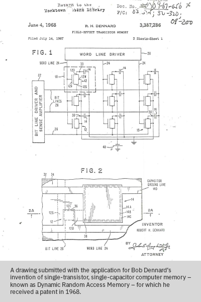
From that insight, Bob Dennard invented dynamic random-access memory, or DRAM.
Dennard’s insight would soon lead to DRAM chips with a kilobit (a thousand bits) of memory. Over the next five-and-a-half decades DRAM would, generation by generation, evolve into an 8-gigabit (8 billion bits) storage medium. Today, 8-gigabit DRAM chips are found in everything from the smartphones in our pockets to the supercomputers that power the global economy. And 16-gigabit DRAM is on the way.
Not only did DRAM memory sweep away the earlier magnetic technologies. It became the foundational technology for an industry that has reshaped human society – from the way we work, to the way we entertain ourselves and even to the way we fight wars. Today, two-thirds of the human population carries Dennard’s invention in their pocket, contained within cellphones or smartphones that are capable of storing movies, thousands of photos and entire music libraries.
This month, Dennard’s career will be celebrated when the Semiconductor Industry Association bestows upon him the Robert N. Noyce Award, the industry’s highest honor.
“With Bob’s invention, we were able to really unleash the capability of programmable computing,” Dr. John E. Kelly III, IBM executive vice president, said recently.
Dennard, in a 2013 speech accepting the prestigious Kyoto Prize in Basic Sciences, recalled the good fortune of IBM’s assigning him the task of translating computer memory to the new silicon-based technology of the 1960s. “I was ready,” he said. “I was working on the right project at the right time, and I knew my mission.”
The Theory that Inspired the Future
Dennard began his career in 1958 as a newly minted electrical engineer with a Ph.D from Carnegie Institute of Technology, now Carnegie Mellon University. He went to work at IBM’s then partially completed Thomas J. Watson Research Center in Yorktown Heights, New York, designed by the neo-futurist architect Eero Saarinen.
 Yorktown Heights was, and remains, the workplace of some of the world’s foremost scientists, electrical engineers and physicists – an intellectual hive where many of IBM’s running total of more than 139,000 total U.S. patents have been hatched.
Dennard’s 1966 invention of the DRAM is not his only lasting mark on the computing world. In 1972, he conceived an idea that had an equally lasting legacy, showing a path forward for the entire semiconductor industry. He sketched out a detailed model, fleshed out in a paper two years later, for his “scaling theory,” now known as Dennard Scaling.
Dennard Scaling predicted that as the dimensions of transistors became smaller, they would become more numerous in a given space, more powerful and cheaper, even as the energy each chip consumed would remain almost constant.
With each successive generation, there would be a doubling of the number of transistors that could fit into a given space, as the operating frequency – known as clock speed – would increase by 40 percent.
In short: As more and more transistors could be packed into ever smaller spaces, computers themselves would get faster and cheaper.
Implicit in this simple set of principles was not only a remarkable economics-of-scale but an entire business ecosystem. Since his 1974 paper, the semiconductor industry has marched forward guided by a steadfast belief in Dennard Scaling, willing to invest hundreds of billions of dollars in the breakthroughs that have led to astounding technical progress.
Companies and entire industries could map their futures on the assumption that every few years, newer and ever more powerful memory and logic chips would be attainable.
Executives in the semiconductor industry readily acknowledge Dennard’s scientific contribution. They also note his willingness to share his wisdom.
“Bob was already a legend the first time I met him when I joined IBM Watson in 1995,’’ said Lisa Su, president and CEO of the chipmaker AMD, who spent more than a dozen years at IBM early in her career. “Besides being a brilliant technologist, he was always willing to mentor and guide young device folks like me.’’
A Golden Age of Technical Progress
The world had been first alerted to the power of scaling by Douglas Engelbart in 1959 in a paper presented at a Philadelphia technical conference. Engelbart, then working at the Stanford Research Institute, realized that shrinking transistors in silicon-based systems would lead to increasingly powerful computing systems. He went on to design technologies that would lead directly to personal computing and the Internet.
Sitting in the audience for Engelbart’s presentation was Gordon Moore, then a 30-year-old chemist who two years earlier had helped found Fairchild Semiconductor Corporation. In 1965 Moore, in an article in Electronics Magazine, noted that the semiconductor industry was “cramming more components onto integrated circuits” at a remarkable rate, at the time doubling the number of transistors that could be etched on a silicon chip at a regular interval of roughly two years.
Soon thereafter, the phenomenon was dubbed “Moore’s Law” by California Institute of Technology physicist Carver Mead, who would proceed to develop new design methodologies that would make it possible to create computing chips with hundreds of thousands of components. The chips of this era are known as Very Large Scale Integrated, or VLSI, circuits.
It would be Dennard, however, who spelled out the math and physics underpinning Moore’s Law and who provided the industry agenda for what IBM Fellow Bijan Davari describes as the “golden age” of scaling that lasted into the early 21st century.
“During that period the frequency of the microprocessor improved 1,000-fold,” Davari said. That in turn created a virtuous circle as more memory and more computing speed made new software applications possible, which in turn created new demands for computing power.
A French-Horn Turning Point
Robert Heath Dennard’s life and career illustrate the power of invention and ingenuity in transforming America from an agrarian society to today’s post-industrial information economy.
Born in 1932, in Terrell, Texas, Dennard spent some of his early years on a farm without electricity and taking his lessons in a one-room schoolhouse. When Dennard was in high school, still in Texas but now living near Dallas, a guidance counselor recommended that he pursue electrical engineering because it was a growing field. He had been planning to join his friends at a local junior college. But then, a recruiter for Southern Methodist University, aware of his talent with the French horn, offered young Dennard a band scholarship. Music and science would ever after be his twin passions.
After SMU came Carnegie Institute and then IBM. It was a time of technological ferment. The transistor had been demonstrated a decade earlier at Bell Laboratories. In 1958, shortly after Dennard’s arrival at Yorktown Heights, Jack Kilby, a Texas Instruments electrical engineer, demonstrated the first solid state electronics device composed of a transistor, a resistor and a capacitor to create a simple oscillator circuit. It was indeed ‘’the right time’’ for Dennard, whose career would parallel the explosive growth of the scientific advances and societal impacts of microelectronics.
“A Willingness to Go Beyond the Rules”
Beyond his inventions and his theories, Dennard would make his mark at IBM by instilling a culture of innovation in the company’s research division. Thomas J. Watson Jr., who led the company from the early 1950s to the early 1970s, referred to employees like Dennard as “wild ducks.” People who refused to “fly in formation.”
 Russ Lange, an IBM Fellow and former IBM Vice President of Technology, who worked with Dennard for many years, said that his wild-duck instincts meant that no challenge was insurmountable.
“You needed a willingness to go beyond the rules, to not be told no by executives,’’ Lange said. ‘’That was a critical aspect to really making progress in this industry. That was the recognition of the wild duck.”
Those qualities are more essential than ever today at IBM – and wherever else researchers continue to push the boundaries of computing. Because, despite the decades-long durability of Dennard’s pivotal theory, the golden age of scaling is now over.
First, around 2006, computer clock speed stopped increasing; nanoscale transistors were nearing such microscopic dimensions that the leakage of electrical current was becoming a vexing challenge. The work-arounds have included a variety of technical breakthroughs, including new types of insulating materials that minimize current leakage and 3-D chip architectures to increase density.
More recently, though, the cost of transistors has stopped falling. That is mainly because of the huge investments required – more than $20 billion – to build silicon foundries capable of making chips with features 10 nanometers and smaller.
In other words, computing’s virtuous cycle of ever faster, ever cheaper chips has slowed to a virtual crawl.
These developments have put a renewed premium on the values that Bob Dennard’s career embodied: human ingenuity and invention. The physical limits of semiconductors, for example, are one reason that IBM is intent on pursuing quantum computing to help solve some of the most specialized kinds of information-processing challenges in coming years.
“Bob, and I would always have lively discussions about whether there was going to be an end to the scaling,” Lange recalled. “And he would say, ‘Yes, there’s an end to scaling. But there’s no end to creativity.’”

Writer-in-Residence at the Stanford Institute for Human-Centered Artificial Intelligence; Former New York Times technology reporter

New Advances in Green IT
What does COVID-19 have in common with climate change? Supercomputers are an important tool in fighting both of them. In collaboration with the White House Office of Science and Technology Policy and the U.S. Department of Energy and many others, IBM helped launch the COVID-19 High Performance Computing Consortium, which assembled massive supercomputing power to […]
IBM’s z15: Built for the Cloud You Want, with the Privacy and Security You Need
As more enterprises embrace a hybrid multicloud strategy, IBM is addressing their most important requirements during this transformation with the new z15, which now features encryption everywhere, cloud-native development, and instant recovery. IBM consulted with more than 100 companies as part of the design and development for IBM’s z15, a secured and highly-resilient enterprise platform. […]
AI Supercomputing and the Enterprise
In June 2008, the well-named IBM Roadrunner supercomputer blew past all competitors by clocking at compute speeds no system on the planet had achieved before. Fast forward 10 years to June 2018. IBM and the U.S. Department of Energy debuted Summit, the world’s smartest and most powerful supercomputer, capable of 200 million calculations, a million […]